Hello, welcome to the Nanjing Innovation Capital Group


Promoting High-Quality Development of the Industrial Chain · Venture Capital Record | Jing Sheng Co., Ltd.: Leading High-Quality Development in the Field of Semiconductor Crystal Material Growth Equipment with Core Technology as the Foundation.
Release time:
2023-09-18
Source:
China is the largest semiconductor market in the world, with chip sales accounting for about one-third of the global market. With the rapid development of artificial intelligence, big data, cloud computing, the Internet of Things, automotive electronics, and consumer electronics, the demand for information technology is increasing. The semiconductor industry, as the lifeblood of the electronic information industry, has also entered the third generation represented by wide bandgap semiconductor materials such as silicon carbide (SiC) and gallium nitride (GaN). Third-generation semiconductor technology plays an important role in modern technology and economic development and is a crucial support for promoting and enhancing the level of "Made in China." However, achieving breakthroughs in technology and industrialization still faces some challenges, primarily in materials, preparation, and processes. "As one of the important links in semiconductor manufacturing and processes, growing single crystals is the foundation for manufacturing high-quality semiconductor devices. The advancement, stability, and compatibility of crystal growth equipment with manufacturing processes have a decisive impact on the performance of material manufacturing." Nanjing Jingsheng Equipment Co., Ltd. (referred to as "Jingsheng Co.") has over ten years of experience in manufacturing semiconductor-grade crystal growth equipment and is a leading domestic enterprise in crystal growth equipment in China. One of the founders and vice president, Zhang Xiaolu, stated that he believes: "Crystal growth equipment is the 'starting point' equipment in the upstream of the semiconductor industry, and the quality of the grown crystals plays a crucial role in chip manufacturing and downstream applications."
In recent years, as domestic applications in new energy, photovoltaics, and other fields gradually establish a dominant position globally, it has also promoted the development of China's semiconductor industry towards self-sufficiency and localized control. The localization rate of equipment and market space has significantly increased. Jingsheng Co. laid out and deeply cultivated the crystal growth equipment field over a decade ago and is one of the few listed companies in China capable of achieving equipment technology verification and mass supply of crystal growth equipment.
Act according to the situation, from 0 to 1
Around 2010, Li Hui, who had experience working in globally leading industrial manufacturing companies, keenly discovered through market changes and industry developments that although China is the world's largest manufacturing country, it has not formed an industrial chain that can support independent design, manufacturing, and packaging in the semiconductor industry. Particularly, the upstream semiconductor crystal growth equipment industry is almost blank, with market demand heavily relying on imports, which will be difficult to sustain the development of emerging industries, especially the information technology industry, and gain international competitive advantages in the long term. Realizing its importance and combining it with a forward-looking judgment of future value, Li Hui resolutely decided to enter the industry. In 2012, with the support of like-minded partners and investors, Li Hui founded Nanjing Jingsheng Energy Equipment Co., Ltd. (the predecessor of "Jingsheng Co.").
The domestic semiconductor industry chain started relatively late, and the crystal growth equipment and semiconductor material manufacturing industries have also developed relatively slowly due to extremely high entry barriers and the need for comprehensive application of knowledge from multiple disciplines and fields. Professional talent is even harder to find. To overcome the difficulties of talent and funding in the initial stage, Li Hui led the team to seek and attract professional talent while strengthening collaboration and coordination with top foreign technical experts, transplanting the most advanced thermal field design and crystal growth control technology into the crystal growth of sapphire materials, achieving breakthroughs in core technologies such as equipment mechanical design, growth processes, and thermal field design. In the same year, the first product, the sapphire single crystal furnace, was launched.
"In 2012, sapphire materials, which are suitable for LED substrate materials, consumer electronics, and military applications, thrived in the global semiconductor industry. However, due to technical limitations, the domestic equipment at that time could only reach about 30 kilograms. Our first sapphire single crystal equipment started at 85 kilograms, which significantly increased the utilization rate of sapphire materials in the machining process, and compared to similar foreign products, the price was nearly halved, thus receiving considerable industry response and allowing the company to establish a foothold in the industry," Zhang Xiaolu recalled.
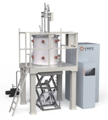
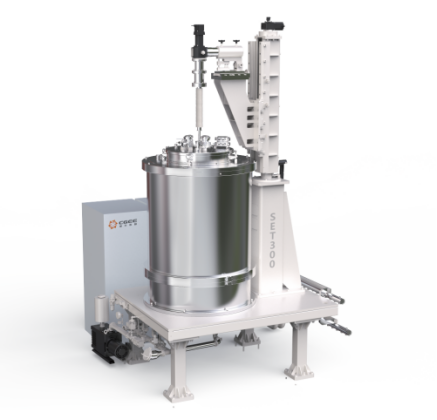
The success of sapphire single crystal equipment in the market alleviated the company's operational pressure and allowed the team more time to refine core capabilities such as thermal field design and crystal growth processes, leading to later products like the SET300, which can be used for large-size sapphire single crystal growth of 300-420KG. In 2014, with the release of the "National Integrated Circuit Industry Development Promotion Outline," "domestic production of large-size silicon wafers" was listed as a key national science and technology project, and Jingsheng Co. welcomed a significant development opportunity.
Technology opens the way, craftsmanship in research and development
To change the situation where chips rely entirely on imports, the production of raw material silicon wafers must first achieve localization. In the silicon wafer manufacturing process, the importance of equipment that can grow qualified crystals in key processes such as crystal pulling, grinding, polishing, and quality control for large-size silicon wafer manufacturing is self-evident. At the end of 2015, guided by national policies and supported by partners, Jingsheng Co. focused on the research and development of 12-inch silicon single crystal semiconductor growth equipment based on the technical homology of high-temperature high-vacuum crystal growth equipment, promoting domestic substitution.
With persistent effort, success is not in vain. In 2016, the first 12-inch semiconductor-grade single crystal silicon furnace was successfully developed, and Jingsheng Co. also engaged in in-depth cooperation with Shanghai Xinxing, a subsidiary of Shanghai Silicon Industry, becoming the only domestic supplier of semiconductor-grade single crystal silicon furnace products, achieving the successful offline of the first 12-inch crystal rod by the end of the year. In 2018, the 12-inch semiconductor-grade single crystal silicon furnace, with a structure design featuring high stability and high reliability, passed acceptance by Shanghai Xinxing, thus breaking the historical blank of domestic production and achieving mass production.
"The mass production of the 12-inch semiconductor-grade single crystal silicon furnace is of great significance not only for the company but also for the important technology and equipment in the industry to achieve domestic substitution." Although research and development is not easy, Zhang Xiaolu believes that this breakthrough has far-reaching significance for promoting the "self-controllable" process of China's semiconductor material sector. "Today, Jingsheng Co.'s semiconductor-grade single crystal silicon furnace is mainly used in the manufacturing of 8-12 inch semiconductor silicon wafers, and can provide customized solutions for the 'crystal growth equipment + process' based on different customer requirements regarding product technical specifications and crystal growth processes, according to key product components such as thermal field structure, crystal growth control system strategy, visual recognition system, magnetic field strength and distribution, and oxide filtering system, up to the 28-nanometer manufacturing stage."
Market rise, advantages highlighted
In 2016, third-generation semiconductor materials represented by silicon carbide emerged and were listed as key development industries by the state. That year was also defined as the "first year of third-generation semiconductor development," and the industry development welcomed a "golden age."
After establishing core competitiveness in the silicon semiconductor field, Jing Sheng Co., Ltd. actively laid out plans and initiated the research and development of third-generation compound semiconductor silicon carbide single crystal furnaces. "Compared to silicon semiconductors, silicon carbide is in a more closed ecosystem. As downstream application demands arise and the industry becomes increasingly refined in its division of labor, domestic silicon carbide substrate manufacturers will need more support from local equipment suppliers. The growth of silicon carbide crystals belongs to a black box growth model, and its characteristics of slow growth rate and low yield lead to high precision requirements for controlling temperature and pressure during the growth process. To increase production capacity, silicon carbide substrate manufacturers need to purchase a large number of single crystal furnaces, which is also an opportunity for the company to forge advantages and achieve rapid development in small steps," said Zhang Xiaolu. Chairman Li Hui keenly captured that silicon carbide would become a new growth point for the company's business, thus establishing a special team internally and introducing talent externally, leading to the official delivery of the first silicon carbide single crystal furnace product in 2018.
Jing Sheng Co., Ltd.'s silicon carbide single crystal furnaces include categories such as PVT induction heating/resistance heating single crystal furnaces and TSSG single crystal furnaces. Among them, the physical vapor transport (PVT) silicon carbide growth furnace has advantages in high-precision transmission, high-precision temperature and pressure control technology, crystal growth visualization monitoring technology, and gas path system optimization design technology, which can effectively improve product yield and shorten crystal growth cycles, mainly applied in the preparation of 6-8 inch silicon carbide single crystal substrates.
"Due to the characteristics of silicon carbide materials and the limitations of the current stage of growth process development, the domestic silicon carbide single crystal furnace growth methods mainly rely on the more mature PVT method, in addition to the liquid phase epitaxy (LPE) method, which has characteristics such as high quality, easy expansion, stable P-type doping, and observable growth processes. Jing Sheng has successfully delivered LPE liquid phase furnaces to customers, and the liquid phase method (LPE) is expected to become a future method for preparing larger size and higher quality silicon carbide single crystals at lower costs," Zhang Xiaolu introduced. It is reported that the company has delivered 8-inch silicon carbide single crystal furnace equipment to multiple customers.
According to the third round of inquiry response opinions from Jing Sheng Co., Ltd. and other publicly available market information, the current domestic production capacity of silicon carbide substrates is about 258,000 to 400,000 pieces per year, and it is expected to achieve multiple growth in the next 2-5 years. Based on the calculations from Founder Securities, the global demand for silicon carbide substrates is expected to reach about 6.29 million pieces by 2026, and the entire industry will continue to be in a state of supply shortage.
From furnace to chain, science and technology innovation listing.
The semiconductor materials and specialized equipment industry has high technical barriers, long research and development cycles, large capital investments, and long downstream verification cycles. Therefore, currently, only a few domestic companies can achieve technical verification of crystal growth equipment and supply in bulk.
Based on years of research and development experience and process accumulation, Jing Sheng Co., Ltd. relies on the ability to optimize the upstream and downstream technologies of the "crystal growth equipment - process technology - crystal materials" industrial chain. On the basis of existing crystal growth equipment business, combined with industry development, actual applications across the entire industrial chain, and the continuously increasing demands of customers, the company enriches product varieties and iterates technology, gaining advantages in certification from early downstream customers, forming a "moat" for the company's development.
In 2020, Jing Sheng Equipment initiated financing to enhance the company's research and development, production, and service capabilities in response to the future expansion of silicon carbide substrates and semiconductor silicon wafers. In 2021, the company attracted the attention of Nanjing Venture Capital Fund as an industry leader and received tens of millions of yuan in funding support and resource assistance. In April 2023, Jing Sheng Co., Ltd. was listed on the Science and Technology Innovation Board of the Shanghai Stock Exchange.
Regarding the successful listing of the invested enterprise, the general manager of the investment department of the venture capital group, Ying Ailing, stated: "Jing Sheng Co., Ltd. has advantages in equipment design, crystal growth processes, and control technologies, solving core problems such as stabilizing crystal diameter during semiconductor-grade single crystal silicon growth, accurately measuring liquid surface distance, locking crystal pulling speed, and fitting process windows. The company has growth potential. We hope to become a 'source of fresh water' for key field science and technology innovation enterprises through investment and post-investment empowerment, helping enterprises coordinate resources and better promote development."
Strategizing for the future, breakthroughs in chips.
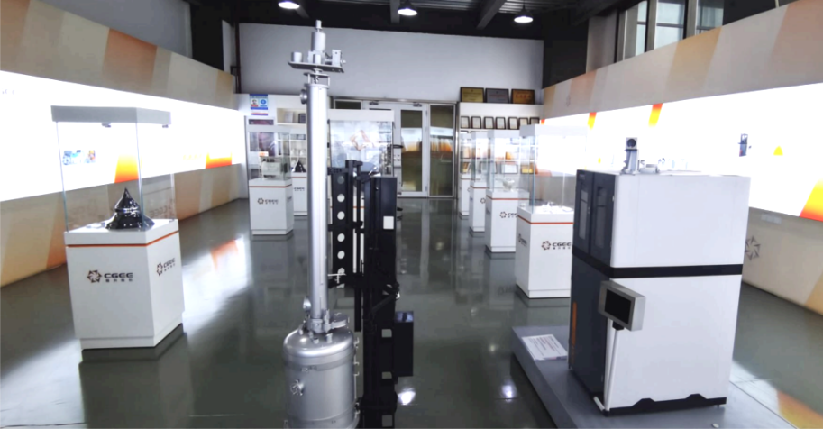
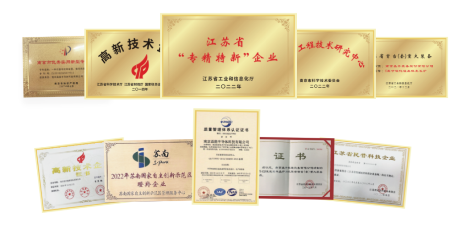
Upholding the values of "integrity and openness, passion and dedication, mutual cooperation and love, humility and progress," Jing Sheng Co., Ltd. has adhered to independent innovation and research and development for more than a decade, maintaining the company's international vision and innovative vitality. Today, the company has a total of 183 employees, has obtained 28 invention patents, 49 utility model patents, and has received national-level honors such as "specialized, refined, and new" small giant and Jiangsu Province's Su Nan National Independent Innovation Demonstration Zone gazelle enterprise. It has been rated as a unicorn cultivation enterprise in Nanjing for two consecutive years, with customers covering domestic leading enterprises or mainstream customers in silicon wafer manufacturing and silicon carbide substrates. The company has established cooperation with well-known enterprises such as Shanghai Silicon Industry (Shanghai Xinxing), Li'an Micro (Jinrui Hong), Shenkong Co., Ltd., Hejing Technology, Sanan Optoelectronics, BYD, and Dongni Electronics, receiving repeat and bulk orders from customers, forming strong advantages in enterprise management, technology research and development, and customer resources in the industry, establishing competitive barriers.
Regarding the development after the company's listing, Zhang Xiaolu believes that as the process of domestic semiconductor material localization accelerates, China will still be the fastest-growing market globally for a period of time. Enterprises in the industrial chain face optimization and enhancement in technology, investment, policies, talent, market, and business cooperation. "Jing Sheng Co., Ltd. will be demand-oriented for semiconductor materials, continuously committed to the research and production of crystal growth equipment, expanding the market share of existing equipment, and actively laying out more product lines. In terms of business, the company will also attempt to go abroad and actively explore markets in parts of Asia and Europe, aiming to become a professional enterprise in crystal material growth equipment with a certain influence in China and even internationally."
Related Annexes

-
Address: 41st and 42nd Floor, Building 4, Financial City, 248 Lushan Road, jianye district, Nanjing City, Jiangsu Province
Telephone:025-86596500
Copyright©2025 NANJING INNOVATION INVESTMENT GROUP CO., LTD

Sweep, pay attention to us
Online Message
Any related questions, please feel free to leave a message